TSMC and NYCU Researchers Demonstrate 0.42-Nanometer Transistor Breakthrough
Key Takeaways
- •The researchers built a monolayer MoS2 top-gate transistor with an epitaxial interface layer only 0.42 nanometers thick.
- •An ultrathin aluminum layer was oxidized into an Al2O3 buffer, which was paired with a hafnium oxide gate dielectric.
- •The dielectric stack achieved an equivalent oxide thickness of about 1 nanometer, a key target for next-generation devices.
- •The fabricated transistors showed low leakage current, minimal hysteresis, and a maximum transconductance of 0.45 mS/μm at around 100-nanometer channel lengths.
- •The findings were published in Nature Electronics and align with broader industry work on 2D channel materials beyond the 2-nanometer generation.
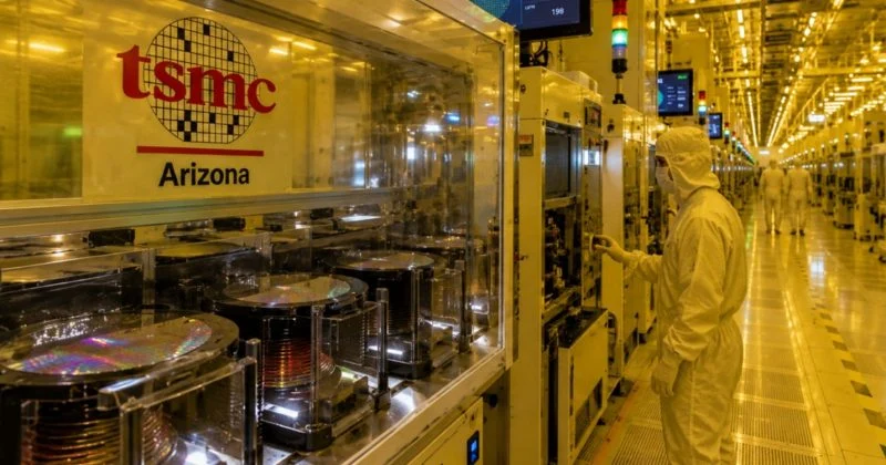
Silicon has served as the semiconductor industry's foundational material for decades, but it is fast approaching physical limits. As transistor dimensions shrink toward the atomic scale, silicon-based designs face fundamental constraints that threaten further miniaturization — and with global demand for compute surging amid the expansion of AI workloads and data-center buildout, the pressure to identify a viable successor material has intensified across the industry. A newly reported advance from TSMC and National Yang Ming Chiao Tung University (NYCU) points to a potential pathway beyond those limits.
The research team fabricated a monolayer molybdenum disulfide (MoS₂) top-gate transistor incorporating an epitaxial interface layer measuring just 0.42 nanometers thick. For context, a single strand of human DNA is approximately 2.5 nanometers wide, making this layer roughly one-sixth that width.
Engineering Around Electron Scattering and Leakage
Two practical obstacles have long hindered the development of working 2D transistors: electron scattering, in which charge carriers deflect off imperfections at the material interface, and leakage current, where electricity flows through unintended paths. The TSMC–NYCU team addressed both by depositing an ultrathin epitaxial aluminum layer onto a monolayer of MoS₂ grown through chemical vapor deposition. They then oxidized that aluminum to form an aluminum oxide (Al₂O₃) buffer.
On top of the buffer, the researchers applied a high-κ hafnium oxide gate dielectric. The combined dielectric stack achieved an equivalent oxide thickness of approximately 1 nanometer — widely regarded as a critical benchmark for next-generation semiconductor devices.
The fabricated transistors exhibited low leakage current and minimal hysteresis, the phenomenon where a device's output lags behind its input signal. Devices with channel lengths of roughly 100 nanometers reached a maximum transconductance of 0.45 mS/μm. Transconductance — the measure of how efficiently a transistor converts voltage changes into current changes — is a key performance indicator, with higher values signaling better operation.
The findings were published in Nature Electronics. The research was led by Dr. Iuliana Radu of TSMC Corporate Research, together with NYCU professors Wen-Hao Chang and Tsung-En Lee.
Why 2D Materials Matter
Two-dimensional materials such as MoS₂ present a promising alternative as silicon scaling runs out of room. The International Roadmap for Devices and Systems (IRDS), the industry body that forecasts semiconductor technology directions, has identified 2D channel materials as leading candidates for transistor nodes beyond the 2-nanometer generation. A monolayer of MoS₂ is naturally about 0.7 nanometers thick, granting it inherently tighter electrostatic control at extremely small dimensions than silicon can provide. Intel and Samsung have also publicly disclosed research programs targeting 2D channel transistors, underscoring that this is a cross-industry effort rather than a single-company pursuit.
Path to Industrial Adoption
Crucially, the MoS₂ in this study was grown using chemical vapor deposition, a technique already deployed at industrial scale. The epitaxial aluminum deposition and oxidation steps likewise do not require fundamentally new categories of manufacturing equipment, which could ease eventual fab-floor integration.
The work aligns with wider industry momentum to bring 2D transistors into mass production. In June 2026, TSMC, imec, and ASML announced collaborative efforts on 300 mm 2D transistor integration — a signal that the leading players in semiconductor infrastructure are treating this material class as a serious candidate for future process nodes.