University of Seoul Student Team Wins Grand Prize at Simulation Challenge 2026
Key Takeaways
- •A University of Seoul student team won the undergraduate grand prize at Simulation Challenge 2026, held at Yeoksam POSCO Tower on July 30.
- •The competition attracted 149 preregistered participants from 18 universities, with 14 teams advancing to the final round across newly introduced undergraduate and graduate categories.
- •The winning team designed a radial collet bonding tool that reduces void formation in hybrid bonding by controlling curvature and contact behavior, a significant challenge in advanced semiconductor packaging.
- •Hybrid bonding is considered essential for high-density packaging applications such as high-bandwidth memory and chiplets, areas where Samsung Electronics and SK Hynix are investing heavily.
- •The grand prize includes a scholarship and the opportunity to present the team's research at Simulation World Korea 2026, the country's largest simulation conference, scheduled for September.
University of Seoul Student Team Wins Grand Prize at Simulation Challenge 2026
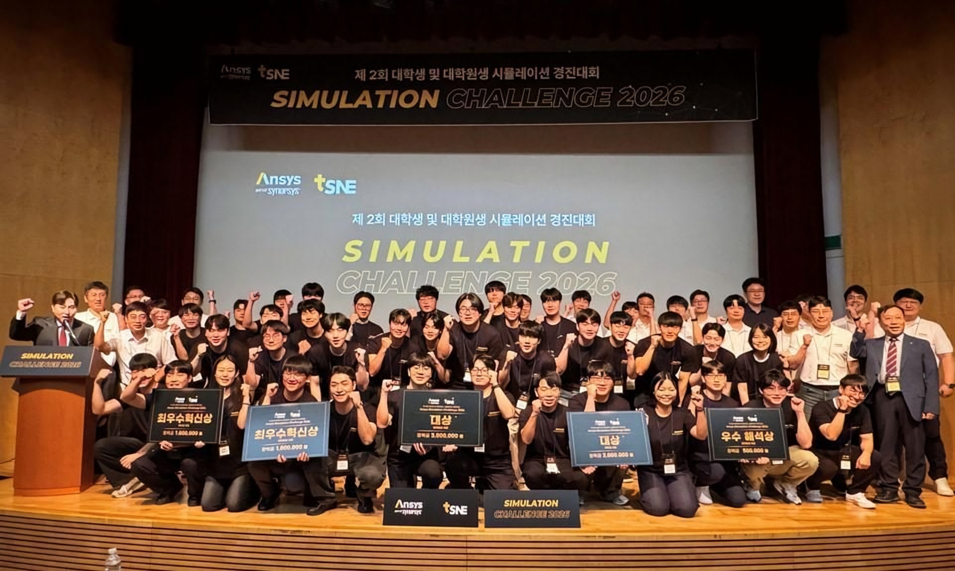
A student team from the University of Seoul has won the grand prize in the undergraduate division of Simulation Challenge 2026, held at Yeoksam POSCO Tower in southern Seoul on July 30.
Competition Overview
The Simulation Challenge, now in its second year, is an academic competition organized by Synopsys Korea's Simulation & Analysis Division and co-hosted by Tae Sung S&E. Participating teams use simulation software to propose solutions to real-world technical industry challenges and demonstrate the feasibility of their designs. The competition reflects a broader industry trend in which South Korean semiconductor companies and their suppliers increasingly rely on simulation-driven design to reduce prototyping costs and accelerate development cycles, particularly as advanced packaging technologies demand tighter tolerances and more iterations than traditional scaling approaches.
This year's edition attracted 149 teams and individual participants during the preregistration period, with 80 teams advancing to the preliminary round. A total of 18 universities from across South Korea participated, including Seoul National University, Korea University, Yonsei University, and the Korea Advanced Institute of Science and Technology (KAIST). For the first time, the competition introduced separate categories for undergraduate and graduate students. Following the preliminary round, 14 teams — six undergraduate and eight graduate — advanced to the final round.
Winning Team and Research
The University of Seoul's winning team, named "Save the World with Hybrid Bonding," came from its Advanced Packaging Lab and competed under the guidance of Park Ah-young, a professor in the Department of Materials Science and Engineering. The team comprised materials science and engineering majors Choi Seung-uk and Jang Sun-woong, along with chemical engineering major Kim Kwon-hee.
The team presented research titled "Design of a Radial Collet Bonding Tool for Reducing Voids in the Hybrid Bonding Process." Hybrid bonding is a technology that directly bonds copper pads and dielectric layers, and it is considered a key enabling technology for high-density semiconductor packaging applications such as high-bandwidth memory (HBM) and chiplets. The technology has drawn heightened industry attention as demand surges for HBM used in AI accelerators, with South Korea's major memory producers — Samsung Electronics and SK Hynix — investing heavily in next-generation packaging capabilities to secure supply agreements with leading GPU designers.
To address the problem of voids caused by trapped air at the interface during bonding, the team proposed a novel bonding tool design that controls the collet's curvature and contact behavior. Through simulations, the team analyzed how the contact area expands sequentially from the center toward the outer edge and examined the pressure distribution at the interface. Based on these results, the team proposed a design approach aimed at reducing the likelihood of void formation. Void defects are a critical yield-limiting factor in hybrid bonding, as even microscopic gaps at the bonding interface can compromise electrical and thermal performance in stacked chip architectures.
The students independently carried out the entire engineering process — from defining the problem and selecting design variables to building the simulation model, analyzing the results, and presenting their findings — demonstrating strong problem-solving capabilities in advanced semiconductor packaging.
Awards and Recognition
The grand-prize-winning team will receive a scholarship and an opportunity to present its research at Simulation World Korea 2026, the country's largest simulation conference, scheduled for September.
"It's meaningful that the students addressed the void problem in hybrid bonding by linking equipment design with simulation and developed a creative solution," Professor Park said.
"It was challenging to venture into the unfamiliar field of simulation, and we went through a lot of trial and error," said Choi, the team leader. "This award would not have been possible without the hard work of our team members and Professor Park's attentive guidance."