South Korean President Lee Jae Myung to Review Progress on Semiconductor and AI Investment Megaprojects
Key Takeaways
- •President Lee Jae Myung chaired a meeting to advance South Korea's three megaprojects, covering major investments in semiconductor production, physical AI, and AI data centers.
- •Senior government officials including Prime Minister Han Seong-sook and top executives from Samsung Electronics and SK Inc. participated in the session.
- •Officials presented plans to secure essential electricity and water infrastructure needed to build the semiconductor production cluster.
- •The initiative aims to distribute investment benefits across all regions of South Korea rather than concentrating them in the capital area.
- •The push comes as global competition in advanced semiconductor and AI technologies intensifies, leveraging South Korea's status as home to the world's two largest memory chip makers.
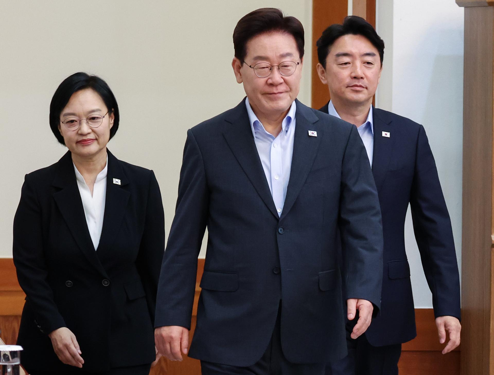
President Lee Jae Myung was scheduled to preside over a meeting on Monday to discuss ways to swiftly implement a large-scale investment initiative for semiconductor manufacturing facilities and artificial intelligence (AI) data centers.
The meeting, set for 2 p.m., is the second of its kind since the Lee administration unveiled its "three megaprojects" in late June. The initiative outlines plans for major investments in a semiconductor production cluster, physical AI, and AI data centers in regional areas across South Korea.
According to the presidential office, Monday's session will focus on measures to support the prompt implementation of the investment plans, as well as strategies to ensure the benefits of the investments are distributed across all regions and throughout the industrial ecosystem.
Attendees will include presidential chief of staff Kang Hoon-sik, presidential policy chief Kim Yong-beom, Prime Minister Han Seong-sook, and government ministers. Top officials from Samsung Electronics and SK Inc. — two of South Korea's largest conglomerates and leading global semiconductor manufacturers — will also participate.
Officials plan to present the progress achieved so far on the investment plans and unveil measures to secure the electricity and water supplies required to build the semiconductor production cluster, the presidential office said. The infrastructure discussion is notable because chip fabs and data centers require large, reliable utility capacity, making site readiness a central issue for turning announced projects into operating facilities.
The meeting follows a Cabinet meeting held at Cheong Wa Dae in Seoul, which President Lee attended alongside Prime Minister Han and chief of staff Kang.
South Korea is home to Samsung Electronics and SK Hynix, the world's two largest memory chip makers, making semiconductor manufacturing a cornerstone of the country's export-driven economy. The Lee administration's push for expanded AI infrastructure and chip production capacity comes amid intensifying global competition in advanced technologies, and the regional focus of the three megaprojects reflects an effort to broaden the reach of those investments beyond the capital area.