Samsung Unveils Industry's First zHBM Concept, Targeting Eightfold Performance Gain Over HBM5
Key Takeaways
- •Samsung unveiled zHBM concept models that vertically stack HBM directly above AI accelerators, moving away from the conventional 2.5D interposer approach where memory sits alongside the processor.
- •Samsung claims zHBM achieves roughly eight times the performance and over ten times the memory density of HBM5 by employing wafer-bonding technology.
- •The architecture reportedly triples energy efficiency and cuts thermal resistance by more than half compared with existing HBM5 designs, addressing a major engineering obstacle in vertical memory integration.
- •zHBM allows customized intellectual property to be embedded in the interlayer between memory and accelerator, enabling customer-specific designs with expanded memory capacity.
- •Samsung presented zHBM as a concept and has not yet disclosed a timeline for commercial production.
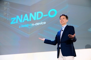
Samsung Electronics Co. has unveiled the industry's first concept models of zHBM, a next-generation memory architecture designed to deliver approximately eight times the performance of HBM5.
The company showcased the new technology at its Future of Memory and Storage 2026 conference, held in Santa Clara, California, on Tuesday local time. Samsung is the world's largest memory chipmaker by revenue and a leading supplier of high-bandwidth memory (HBM) used in AI accelerators, alongside rivals SK Hynix and Micron Technology. HBM has become a critical differentiator in the AI hardware supply chain, with demand surging as cloud providers and chipmakers race to build more powerful training and inference systems.
Designed specifically for advanced artificial intelligence computing, zHBM introduces a fundamentally new memory architecture that vertically stacks HBM directly above AI accelerators. This represents a departure from conventional designs, in which HBM chips are positioned alongside the processor on a package using 2.5D interposer technology. As AI models scale, the data transfer bottleneck between processors and memory — often referred to as the memory wall — has become a primary constraint on system performance, making architectural innovations at the package level increasingly important.
According to Samsung, zHBM employs wafer-bonding technology and can achieve more than 10 times the memory density of HBM5. The architecture also triples energy efficiency and reduces thermal resistance by more than half compared with existing HBM5 designs. Managing heat dissipation has been one of the central engineering challenges in stacking memory tiers, and Samsung's claim of significantly reduced thermal resistance addresses a known obstacle to deeper vertical integration.
The technology further supports customer-specific designs by allowing customized intellectual property to be integrated into the interlayer between the memory and the AI accelerator. This capability expands available memory capacity and improves overall accelerator performance.
By minimizing the physical distance that data must travel between the AI processor and memory, zHBM is engineered to deliver higher bandwidth and greater power efficiency. Samsung said this enables the ultra-fast data processing required for large-scale AI training and inference workloads.
Building on its close collaboration with customers, Samsung Electronics said it plans to further optimize the integration of AI processors and memory through zHBM to maximize overall AI system performance. The company disclosed zHBM as a concept, and it has not yet announced a commercial production timeline. (Yonhap)