Huawei's New Chip Signals China's Strategy to Bypass the Lithography Gap
Key Takeaways
- •Huawei's Kirin 9050 Pro, which the company says contains no US technology, powers its $2,979 Mate XT2 tri-fold smartphone and delivers 42% higher performance than the previous year's model.
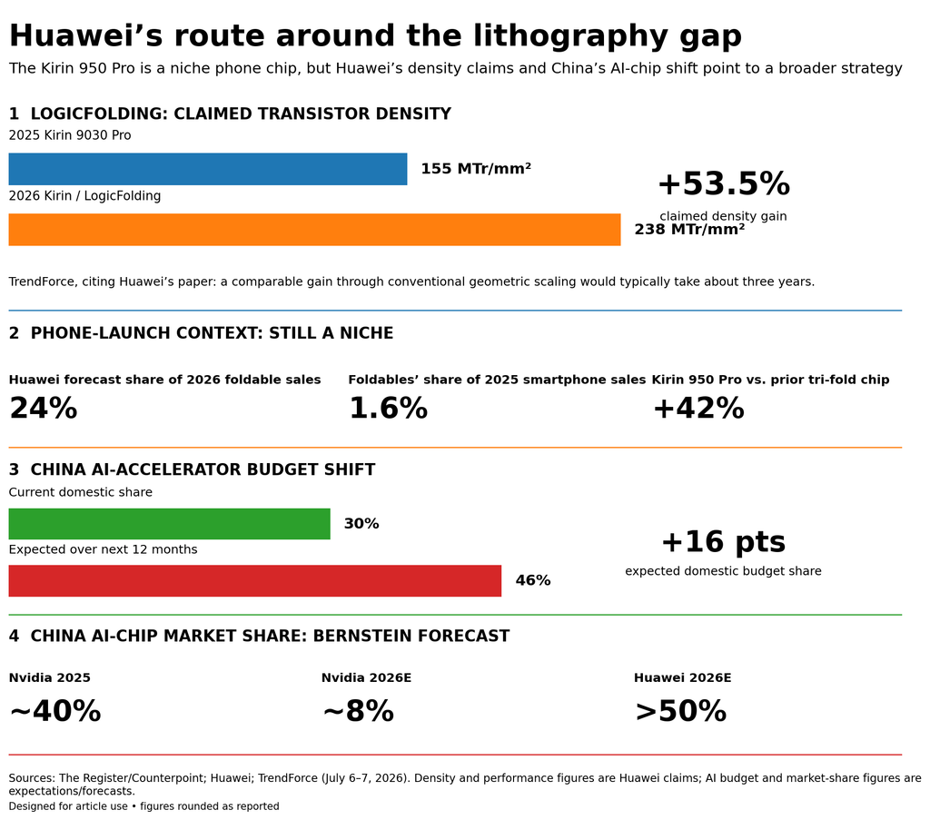
- •Huawei's Tau Scaling Law and LogicFolding approach raised transistor density by 53.5%, results the company says would take about three years to achieve through traditional geometric scaling.
- •ASML has never been permitted to export EUV lithography machines to China, leaving China's most advanced proven manufacturing capability at roughly 7nm, so Huawei is using architecture rather than only smaller transistors to close the gap.
- •Bernstein expects Nvidia's share of China's AI chip market to fall from about 40% in 2025 to roughly 8% in 2026, while Huawei's share rises to over 50%.
- •Huawei still must demonstrate competitiveness in yield, heat management, cost, and volume before it can be considered a match for TSMC's cutting-edge processes.
Huawei has introduced a new smartphone chip that the company says contains no technology from the United States, underscoring its strategy to narrow the gap between China and the rest of the world in semiconductor production despite restricted access to the industry's most advanced tools. The rollout of the Kirin chip matters less for its current market performance than for what it reveals about Huawei's plans relative to companies such as Nvidia, TSMC, and ASML. It is the latest step in a trajectory that began drawing global attention in 2023, when Huawei's Mate 60 Pro shipped with a domestically fabricated 7nm-class Kirin processor despite US sanctions, and US export controls dating to 2019 first cut Huawei off from Google services and advanced American chip technology.
A chip Huawei calls entirely its own
Huawei has installed the Kirin 9050 Pro in its Mate XT2 tri-fold smartphone, which is priced at $2,979. According to reports, Huawei developed the LinxiCore CPU cores, GPU, and NPU used in the Kirin 9050 Pro itself, and it achieved a performance increase of 42% over the previous year's tri-fold phone. The chip is believed to be fabricated by SMIC, China's largest contract chipmaker, using equipment and processes available within China.
The launch also highlights Huawei's push to build its own technology ecosystem. HarmonyOS, Huawei's proprietary operating system positioned as an alternative to Android, has appeared on 85 million devices since launching in October 2024.
The smartphone remains a niche product. Counterpoint projects that Huawei will hold 24% of the foldable phone market by 2026, while foldable handsets accounted for only 1.6% of the smartphone market last year. That makes the launch more significant as a technology showcase than as a volume threat.
Time instead of smaller transistors
On May 25, Huawei unveiled its Tau Scaling Law at the IEEE ISCAS event in Shanghai, as detailed in the company's official announcement. Rather than focusing primarily on transistor miniaturization, the new approach is based on minimizing signal propagation time between devices, circuits, chips, and systems. Huawei describes LogicFolding as the circuit-level implementation of the technology, involving active stacked layers and shorter connecting wires. The framing echoes the industry's familiar Moore's Law debate: as transistor shrinking grows harder and more expensive at each node, packaging and architecture — areas where 3D stacking is already mainstream at TSMC, Samsung, and Intel — have become the industry's other lever for continued performance gains.
According to TrendForce, citing Huawei's updated article, transistor density has increased from 155 million to 238 million transistors per square millimeter — a 53.5% increase. Huawei says achieving comparable results through traditional geometric scaling would require approximately three years of development. The company also claims that 381 chips have been developed and mass-produced using the Tau principles over more than six years.
"I can confidently say in the coming 10 years our solutions for mobile computing and AI computing will be competitive," He Tingbo said.
Betting around ASML's machines
Huawei's 2031 target is not a promise to fabricate a true 1.4nm process. The company says future high-end chips could reach transistor density equivalent to a 1.4nm process. TSMC plans 1.4nm mass production in 2028, while China's most advanced proven manufacturing capability is still widely viewed as about 7nm. The constraint is rooted in equipment: ASML, the Dutch company that is the sole maker of EUV lithography machines, has never been permitted to export them to China, as the Dutch government withheld licenses under pressure from Washington and later restricted advanced DUV shipments as well.
Nor has Huawei abandoned lithography. The company is reportedly investing in domestic producers of advanced DUV technology and other equipment. Architecture, therefore, is one route to filling the tool gap, not a substitute for manufacturing progress.
Why Nvidia should be watching
AI represents a larger opportunity. Huawei is set to extend its LogicFolding technology into its Ascend accelerators, with the Ascend 990 anticipated to be available in 2030. Chinese cloud and AI firms, including many building large language models, have already turned to Ascend and other domestic accelerators as US rules restrict access to Nvidia's most advanced GPUs, which is exactly the demand base Huawei's roadmap is aimed at.
According to a survey, Chinese executives expect local brands to account for 46% of the total AI-accelerator budget in the upcoming year, up from 30%. According to Bernstein, Nvidia's share of the AI chip market in China is expected to drop from around 40% in 2025 to approximately 8% in 2026, while Huawei's share will rise to over 50%.
Policy is accelerating this transition. According to CSIS, export controls imposed by the US and allied powers have sped up China's localization efforts even as they limit the reach of sophisticated technologies. Cryptopolitan has also noted that Nvidia's H200 return to China comes as local players continue to gain market share.
The impact extends well beyond phones. The Semiconductor Industry Association predicts that $4 trillion or more will be spent on AI data-center infrastructure before 2028, with semiconductors accounting for as much as $2.8 trillion. If a larger share of that spending goes to Chinese chips, it could affect the global accelerator market before China fully closes its manufacturing gap.
The gap that architecture can't close yet
Huawei still needs to demonstrate capability in yield, heat management, cost, and volume. The new Kirin shows that strong design can help overcome some manufacturing limitations, but it does not yet prove the company can compete with TSMC's cutting-edge process. Watch points going forward include whether SMIC's domestic toolchain can scale advanced production, whether Huawei's Ascend roadmap ships on schedule, and how US and allied export policy responds as Chinese alternatives gain share.
The key takeaway is strategic. China is attempting to use its limited access to foreign tools to create demand and to leverage capital and engineering expertise in building its own semiconductor industry. If China succeeds, foreign suppliers including Nvidia will feel the consequences before China manages to advance its lithography capabilities.
